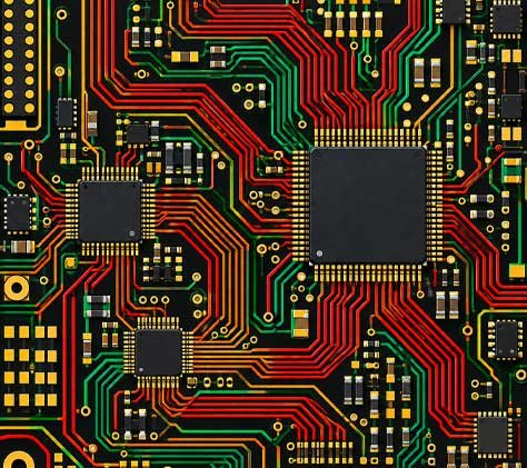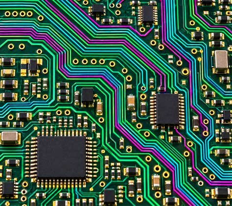



Advance PCB Design Course

ADVANCED PCB TRAINING • LAHORE

Advanced PCB Design Course

Master professional PCB design, multilayer PCB layout, high-speed routing, DRC,

signal integrity and manufacturing-ready design techniques with our hands-on

Advanced PCB Design Course in Lahore.

This course is designed for engineering students, electronics learners and professionals who want practical PCB designing skills using industry-standard tools and real-world projects.

8 Modules

Comprehensive curriculum

24+ Lab Hours

Hands-on practice

1 Advanced PCB Project

From concept to working board

Certificate

Upon completion Boost your career
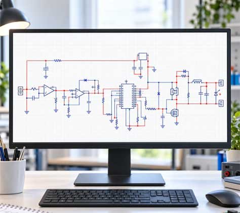
Design Like a Professional

Learn the complete professional PCB design workflow from schematic

capture and component placement to advanced routing, DRC, signal integrity and manufacturing output.

Schematic Capture

PCB Layout

Advanced Routing

Manufacturing Output

What You Will Master

Gain practical skills and industry knowledge through a structured, hands-on curriculum.

Multilayer PCB Design

Design complex multilayer boards with proper stackup and layer planning.
High-Speed Routing

Learn differential pairs, impedance control, and signal integrity basics.

Design Rules & DRC

Set up and use design rules to create error-free layouts.
Power & Ground Planes

Design robust power distribution networks for reliable performance.
Gerber & ODB++ Files

Generate and verify manufacturing files for real production.

Design for Manufacturing

Apply DFM guidelines for cost-effective, reliable boards.

Course Curriculum

Eight practical modules designed for real-world skills.

LEARN TODAY 

BUILD TOMORROW 

Advanced Schematic Design

Create clean, professional schematics using proper project structure, component connections, net labels, annotations, and electrical rule checks.

Component Libraries & Footprints

Learn how to create and verify component symbols, PCB footprints, pin mapping, pad sizes, and manufacturer datasheets.

PCB Stackup & Layer Planning

Understand multilayer PCB construction, signal layers, ground planes, power planes, dielectric materials, and controlled-impedance planning.

Placement, Routing & Copper Pours

Master professional component placement, trace routing, vias, copper pours, thermal reliefs, grounding, and return-current paths.

High-Speed & Differential Pair Routing

Learn differential-pair routing, length matching, routing constraints, impedance control, and techniques to reduce signal noise.

DRC, Signal Integrity & EMC Basics

Use design-rule checks to detect PCB layout issues before manufacturing. Learn the fundamentals of decoupling, grounding, EMI, EMC, and signal integrity.

Gerber, ODB++ & DFM Review

Generate and verify manufacturing files including Gerber, drill, pick-and-place, BOM, and ODB++ outputs. Apply DFM checks before fabrication.

Final Advanced PCB Project

Complete a production-ready PCB design project that demonstrates your layout, routing, verification, and manufacturing-documentation skills.

Next Batch

Get practical PCB design training with professional software, lab access, small-batch learning and direct instructor support.

Hands-on lab access

Small batch size

Certificate upon completion

Get in touch for upcoming dates
Advance Your Skills with Our Advanced PCB Designing Course

Join our Advanced PCB Design Course in Lahore and gain practical skills in

multilayer PCB design, high-speed routing, DRC, DFM, signal integrity and

manufacturing-ready PCB development.

  • Learn advanced PCB design with industry-standard tools
  • Design real multilayer boards, copper pours, and differential pairs
  • Build a portfolio-ready advanced PCB project

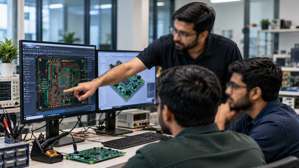
Learn Advanced PCB Designing in a Real Electronics Lab

Get hands-on experience in our professional electronics lab in Lahore. The Advanced PCB Designing Course helps you move beyond theory by working with real PCB layouts, design tools, routing techniques, and manufacturing-ready files under expert guidance.

Practical PCB design demonstrations

Professional PCB design tools

Direct instructor feedback

Ahmad Raza — Lahore
Ahmad Raza — Lahore@username
“Excellent hands-on course. I learned PCB design, fabrication, and testing step by step. The practical lab work made everything much easier to understand.”
Ayesha Khan — Lahore
Ayesha Khan — Lahore@username
“The instructors explained every concept clearly and gave personal guidance during the practical sessions. I now feel confident designing my own PCB layouts.”

Usman Ali — Faisalabad
Usman Ali — Faisalabad@username
“Very professional training environment with real tools and equipment. The final project helped me build a strong portfolio piece.”

Frequently Asked Questions

Do I need prior PCB design experience?

Basic electronics and schematic knowledge is helpful. This advanced course is ideal for learners who want to move from basic layouts to professional PCB design workflows.

Which software will I use?

You will learn using professional PCB design tools and industry-standard workflow practices for schematic capture, layout, routing, DRC, and manufacturing output generation.

Is this an on-campus PCB design course in Lahore?

Yes. The course is conducted in Lahore with hands-on lab access and instructor guidance.

TAKE THE NEXT STEP

Ready to Master Advanced PCB Designing?

Join our Advanced PCB Designing Course in Lahore and gain practical skills in

multilayer PCB layout, high-speed routing, DRC, Gerber files, and manufacturing-ready design.

About Us

The argument in favor of using filler text goes something like this: If you use real content in the Consulting Process, anytime you reach a review point you’ll end up reviewing and negotiating the content itself and not the design.

Contact Info